Nanoscale Techniques for Characterizing Gemstone Coatings: A Case Study on Synthetic Moissanite

ABSTRACT
This study investigated the application of colored coatings on synthetic moissanite, a process aimed at simulating the appearance of rare blue and pink diamonds. The analysis focused on characterizing colored coatings on commercial synthetic moissanite and uncovering the possible techniques used. By employing a range of nanoscale analytical methods (including Auger electron spectroscopy combined with argon ion beam sputtering, spherical aberration–corrected transmission electron microscopy with electron energy loss spectroscopy, and electron probe microanalysis), the compositions and thicknesses of the coatings were determined, revealing their nanoscale thin-film properties. These films varied in composition, leading to the distinct blue and pink hues observed for the synthetic moissanite samples. The suite of analytical techniques presented in this study offers a robust basis for characterizing colored coatings on a variety of polished gemstones, providing compelling evidence of the fabrication principles and mechanisms behind these coatings.
People have always loved the rich colors of natural gemstones. Owing to the development of advanced technologies, there are now a variety of processing techniques to enhance and alter these colors, such as heat treatment, radiation treatment, and lattice diffusion (McClure and Smith, 2000). Coating technologies are also used to change the appearance and color of gemstones, and these have evolved significantly over time. Ancient civilizations such as the Egyptians and Romans used natural dyes and oils to enhance gemstones. During the Middle Ages and beyond, from the Renaissance period to the eighteenth century, the application of metal oxides and foil backing techniques emerged. The introduction of electroplating technology in the nineteenth century revolutionized coating, enabling the deposition of thin metal layers on gemstones. The development of chemical vapor deposition (CVD) and physical vapor deposition (PVD) in the latter half of the twentieth century truly transformed the scope of gemstone coating, achieving precise and durable enhancements (Nassau, 1984; McClure and Smith, 2000; Breeding et al., 2010). Continual technological advancements have enabled coatings to be applied to a wide range of gemstones, including diamonds (Shen et al., 2007), topaz (Schmetzer, 2008), tanzanite (Cooper and Renfro, 2014), jadeite jade (Zhang et al., 2013), and synthetic cubic zirconia (Shigley et al., 2012).
Synthetic silicon carbide (SiC, known as synthetic moissanite) entered the gemstone market around a quarter of a century ago (Nassau et al., 1997). It gained a large market as a diamond imitation because some of its physical properties, such as refractive index, hardness, and specific gravity, are similar to those of natural diamond. Unlike diamond, synthetic moissanite is not cubic. Therefore, the simplest means of distinguishing it is the doubling of facets. Synthetic moissanite has many applications, including abrasives and the fabrication of semiconductors (Elasser and Chow, 2002; Friedrichs et al., 2011; Liu et al., 2015). The structure of large single-crystal SiC used as gem material is mainly 4H-SiC and 6H-SiC (α-SiC, polytype, hexagonal) (Li and Bradt, 1986; Nassau et al., 1997; Chen et al., 2008; He and Shen, 2020).
Rare blue and pink diamonds have always been expensive, so these two colors are often seen in imitation diamonds. To date, colored synthetic moissanite has been produced by modifying the crystal structures or doping with trace elements during the production process. For example, the 3C-SiC structure (β-SiC, polytype, cubic) is yellow, while n-type α-SiC doped with nitrogen and p-type α-SiC doped with aluminum give colors such as light brown, green, and deep blue (Chen et al., 2008; He and Shen, 2020). However, doping methods have not yet achieved synthetic moissanite with light blue and pink colors similar to those encountered in colored diamonds. Although such colors can be produced by a coating process, coated gems are not widely accepted in the market.
This study applied characterization techniques common within the materials science community to analyze the type of coating found on the colored synthetic moissanites as well as the possible processing technology used to produce the coating.
BACKGROUND
As a diamond substitute, synthetic moissanite has acquired a certain market share because it is affordably priced. With the increase in production capacity, the market price of colorless material has fallen drastically in recent years. However, when pink and light blue coated synthetic moissanite initially entered the market, their prices were several times higher. When gem laboratories receive samples of colored synthetic moissanite, most producers and sellers claim they are not coated. On one occasion, the Tai-Da Gem Research Laboratory in Taiwan received a pink synthetic moissanite, and the seller insisted that the color was not from a coating. However, microscopic observation revealed an uneven distribution of color on the surface of the gem (figure 1A), similar to the phenomenon described by Delaunay (2018). Unlike the samples in the present study, the images provided in that study showed additional golden spots described as “metallic flakes on the surface,” and it was concluded that the pink gem was color-coated synthetic moissanite. Later, the laboratory received a light blue synthetic moissanite that did not show these characteristics under microscopic observation. A difference in luster between the upper and lower portion of the pavilion facets was observed, along with a bronze-colored hue under reflected light (figure 1, B and C) similar to that of coated tanzanite described by Cooper and Renfro (2014) and coated diamond described by Shen et al. (2007).
Furthermore, GIA’s Carlsbad laboratory reported a light greenish blue synthetic moissanite in which the color originated from the bulk crystal itself (Tsang, 2017). A pink color-coated synthetic moissanite was analyzed and reported by the Laboratoire Français de Gemmologie (LFG) in Delaunay (2018). However, these two reports described characteristics that were different from the light blue and pink samples mentioned above. In addition, there was an instance of black synthetic moissanite used to imitate black diamond (Moe et al., 2013).
To avoid damage during examination, nondestructive testing methods are typically used. Some methods commonly used in gem laboratories are Raman spectroscopy, Fourier-transform infrared (FTIR) spectroscopy, ultraviolet/visible/near-infrared (UV-Vis-NIR) spectroscopy, energy-dispersive X-ray fluorescence (EDXRF) spectroscopy, and laser ablation–inductively coupled plasma–mass spectrometry (LA-ICP-MS) (Breeding et al., 2010). However, these conventional testing methods are usually not sufficient to conclusively identify the most recent coatings and other treatments that have come from the materials engineering sector, such as the advanced coating used extensively to produce topaz of various colors. Identifying and characterizing these types of coatings poses a challenge for gemological laboratories. The previously observed results mentioned earlier highlight the limitations of standard gemological equipment. Gabasch et al. (2008) performed experiments using X-ray photoelectron spectroscopy (XPS) to analyze the thickness and composition of the coating on color-coated pink topaz. The study revealed that the coating comprised silicon dioxide as a surface layer and gold as an interfacial layer, with a total coating thickness of approximately 400 nm. Relying on a single analytical technique may not be sufficient to reveal the properties of gemstone coatings, because each method has strengths and limitations. Multiple methods may be necessary to achieve a more comprehensive and accurate evaluation.
Owing to the advancements made in the semiconductor industry and nanomaterial technology, the sensitivity and accuracy of available analytical instruments have improved significantly. The National Science Council in Taiwan has even established a Valuable Instrument Center to coordinate these instrument resources and make them available to the public. In addition to faculty and students from educational institutions, external organizations can access the instruments after completing the required training. The equipment used in the present study was made available to us through this process.
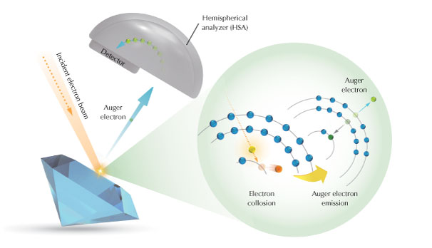
We mainly used Auger electron spectroscopy (AES) to analyze the coatings of pink and light greenish blue synthetic moissanite. This method is suitable for the nanoscale analysis of elemental components and sufficiently sensitive for surface analysis (box A). AES is generally used to analyze components such as coatings, thin films, and oxide layers in machines such as generators and motors, as well as materials used in electronics, semiconductors, and materials science. To the best of our knowledge, this study presents the first application of AES in gemology. Other detection methods used in this study included spherical aberration−corrected transmission electron microscopy (AC-TEM) with electron energy loss spectroscopy (EELS) and electron probe microanalysis (EPMA). These methods were used to obtain micro-longitudinal profiles and images of element distribution, for the qualitative and quantitative analysis of the elements in the surface coating.
MATERIALS AND METHODS
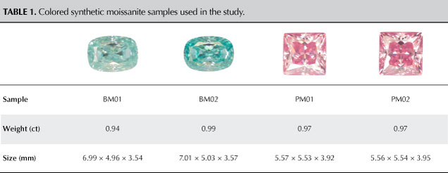
Materials. For this study, two pink, two light greenish blue, and one colorless synthetic moissanite sample typical of those encountered in the lab were purchased in 2020 from the same supplier (Tian Shi Zhi Yue company), which sourced the material from a growth facility in Guangxi Province, China. The four colored samples are shown in table 1.
Methods. The light greenish blue and pink samples were cut along the girdle using a conventional gem saw to separate the crown from the pavilion.
In many surface analysis methods, the user must select possible elements in advance, especially trace elements. EDXRF analysis was performed with a Rigaku EDXL-300 using the standardless fundamental parameter detection method. This method is advantageous in that it quickly analyzes and filters the major and trace elements in a sample. Although EDXRF has a large analytical margin of error for trace elements, it is useful for the preliminary screening of experimental samples. The light greenish blue, pink, and colorless synthetic moissanite samples were tested by EDXRF and the differences in the chemical compositions were analyzed.
In this study, a JEOL JAMP-9510F AES instrument was used with a hemispherical analyzer (HSA) system. HSA is widely used with AES, XPS, and ultraviolet photoelectron spectroscopy methods to obtain electronic energy spectra. Furthermore, HSA combined with argon ion beam sputtering (AIS) is used to ablate the surface of the sample to conduct depth-profile analyses. We used an incident electron beam energy of 10 keV, current of 10.4 nA, and sample tilt angle of 30°. The sputtering energy of the argon ion beam of 2 keV and scan rate of 22.2 nm/min (3 s/cycle) were set based on a standard sample of silicon dioxide. The spatial resolution of AES with AIS was 1 nm. The vacuum pressure of the sample chamber was below 1 × 10⁻⁶ Pa.
Furthermore, high-resolution TEM imaging and elemental analysis of a micro-sectional profile (JEOL JEM-ARM300F Grand Arm AC-TEM with EELS) and elemental analysis and surface-plane mapping (Shimadzu EPMA-8050G high-resolution field-emission EPMA) were performed. A significant feature of AC-TEM is the use of spherical aberration correction to obtain a higher image resolution (Tanaka, 2008). Before TEM experiments, the samples were coated with carbon and platinum as conductive and protective layers, which were identified as the outermost layers in the TEM images. Focused ion beam (FIB) milling was used to prepare lamellae (thickness <100 nm) for TEM analysis. The TEM sample was transferred onto a copper bracket. The operating voltage of the TEM was 300 kV, and the resolution in the high-resolution configuration was 0.063 nm. EELS spectra were obtained in TEM imaging mode, with an energy resolution of 0.8–1.5 eV. The spectral sampling rate was 8000 spectra/s. The vacuum pressure in the sample chamber was maintained below 1 × 10⁻⁸ Pa.
In this study, the EPMA surface images were obtained in backscattered electron (BSE) mode. Throughout the experiment, the electron-beam accelerating voltage and current were set at 15 keV and 10 nA, respectively. A mapping resolution of 50 nm was achieved, with a compositional resolution of 0.1 at.%. The vacuum pressure in the sample chamber was kept below 6 × 10⁻⁴ Pa.
We employed several techniques used in the materials science field, including AES, FIB sample preparation for TEM, AC-TEM with EELS analyses, and EPMA. All these methods require high-vacuum conditions, with the evacuation process requiring approximately 10–15 min. The total analysis time includes the time taken for sample positioning, actual analysis, and removal of the sample from the instrument. The entire process, from initiation to sample retrieval, required approximately 3 h for AES/AIS. For TEM analysis, the process of positioning, carbon and platinum coating, FIB preparation of the TEM lamellae, and sample analysis took approximately 4 h. The duration for EPMA analysis varies depending on the scanning area; for example, evaluating three elements over a 500 × 500 μm area takes about 1.5 h.
It should be noted that some sample preparation methods permanently damage the gemstone. For example, TEM analysis requires coating the samples with carbon and platinum, which remain on the surface. Additionally, AES/AIS and FIB preparation of TEM lamellae result in permanent pore features on the sample surfaces.
These methods analyze a microscopic region of a sample and are only suitable for the detailed examination of individual gemstones to provide critical information about the material characteristics. AES allows for point analysis and can be combined with AIS for depth profiling; TEM analyzes microscopic cross sections of samples; and EPMA provides point, line, and planar mapping analyses.
RESULTS
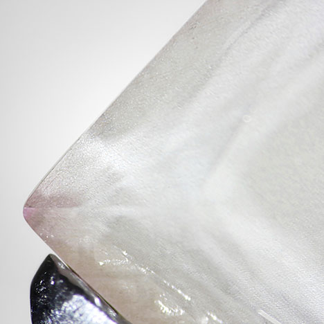
After the light greenish blue and pink samples were cut along the girdle and examined without magnification, we observed that the color was concentrated on the outer edge and the samples were colorless in the middle (figure 2). The coating was applied to all facet surfaces. Furthermore, the EDXRF results (overall averages of the entire colored samples) were compared with those of a colorless sample (CL01). Compared to CL01, the light greenish blue samples had higher concentrations of vanadium, cobalt, and manganese, while the pink samples had a higher concentration of gold. None of these elements were detected in CL01 (table 2). Vanadium, cobalt, and manganese were assumed to be present as coloring agents on the light greenish blue synthetic moissanite, while gold is very common in pink and red coated examples (Yu et al., 2005; Shen et al., 2007; Gabasch et al., 2008).


AES was performed as a function of depth from the surface during AIS. These results showed that the oxygen and vanadium contents on the light greenish blue samples (BM01 and BM02) decreased rapidly at depths of 38 and 54 nm, respectively, while the concentration of carbon and silicon increased rapidly at similar depths. Comparing the surface and bulk regions, the concentrations of oxygen and carbon changed by a factor of ten (in opposite directions), silicon increased by ~12%, and vanadium decreased from a maximum value of 7.15% (BM01) and 6.41% (BM02) to below detection limits in the bulk region (figure 3). Cobalt and manganese were not detected by AES analysis because it was difficult to separate the weak signals from background noise. We concluded that the coatings on samples BM01 and BM02 were silicon dioxide films doped with vanadium, cobalt, and manganese with thicknesses of approximately 45 and 62 nm, respectively, defined by the crossover points where the concentrations of carbon and oxygen were identical (31.27% and 31.52%, respectively).
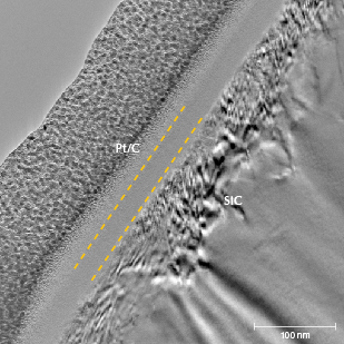


The images of sample BM01 analyzed by AC-TEM with EELS confirmed the AES experimental results. An amorphous silicon dioxide layer with a thickness of approximately 45 nm was observed on top of the SiC matrix. In addition, a damaged SiC layer was observed between the substrate and coating layer (figures 4 and 5). The EPMA map of BM01 confirmed an uneven distribution of small amounts of vanadium, cobalt, and manganese in the coating (figure 6).

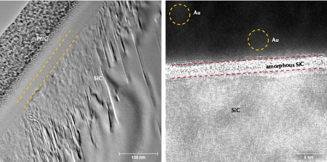

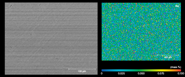
For the pink samples, PM01 did not show the expected AES result and is not presented in the results but discussed later. For sample PM02, it was observed that the thickness of the gold-containing layer was less than 20 nm. In addition, the concentration of gold decreased rapidly from the surface to a depth of ~15 nm, and the concentration in the 15–20 nm depth range was very close to that of the background. The atomic concentration of gold was very low, and it was distinguished by comparing it against the concentrations of the main elements with lower atomic concentration (i.e., silicon) (figure 7). In AES analysis or similar surface analytical techniques, atomic percentages (at.%) refer to the relative content of each element within a designated area compared to the total concentration of all analyzed elements—i.e., the sum of the atomic percentages of all analyzed elements equals 100%. Only the curves for the major element silicon and the trace element gold are plotted in figure 7 (right), to enable easier analysis of the distribution of gold (with low concentration) without interference from other curves. Despite the low concentration of gold, this comparative analysis allowed us to effectively highlight the presence and variations of gold. The AC-TEM images of PM02 also showed an amorphous SiC film on the SiC substrate with a thickness of approximately 3–5 nm (figure 8, left and right), which is consistent with the AES results. However, EELS analysis of the area did not identify the presence of gold (figure 9). The EPMA map of PM02 confirmed that the coating was uneven and contained gold (figure 10).
DISCUSSION
Detection of Trace Elements. AES analysis detected gold for PM02 but not PM01. Because the thin gold-containing coating had a low concentration and uneven distribution of gold, the gold content at the test point of sample PM01 was lower than the detection limit of the AES method (0.1 wt.% for most elements). Because the gold concentration was higher at the test point of sample PM02 than in PM01, trace amounts of gold were detected. The atomic numbers of vanadium, manganese, and cobalt are 23, 25, and 27, respectively; therefore, at the same concentration, vanadium has a slightly higher probability of generating Auger electrons than manganese and cobalt. However, the EPMA mapping results of BM01 showed that these elements had a similar concentration. With a low concentration and large atomic number, it is difficult to detect manganese and cobalt in the synthetic moissanite coating using AES.
The EELS method is similar to AES but has a better resolution for lighter elements. Theoretically, EELS can analyze the elements from carbon to 3d orbital transition metals. Due to the lower resolution for elements with larger atomic numbers, a higher concentration is required to detect these elements (Ahn, 2006). Therefore, the EELS method is suitable for obtaining analysis images of the main elements in the coating, such as silicon, oxygen, and carbon. But because the trace elements (vanadium, manganese, and cobalt) in the coating of BM01 have large atomic numbers and low concentrations, the obtained data is extremely difficult to analyze.
The same problem was encountered for PM02 because gold is a heavy element and not easy to identify using EELS at low concentration. In this case, the EPMA mapping results provide strong evidence that the coating on sample BM01 contained vanadium, manganese, and cobalt, and that the coating on sample PM02 contained gold. The uneven distribution of vanadium, manganese, and cobalt in the film on BM01 was presumably due to the ion implantation technique used to dope these trace elements into the colorless silicon dioxide coating to add color.
Colorization of Coated Synthetic Moissanite. Light Greenish Blue. The thin-film technology used to fabricate SiC and SiO2 coatings is very mature, and there have been many related studies (e.g., Afanasev et al., 1997; Kim et al., 2016; Li et al., 2017; Liu et al., 2019, 2020; Kobayashi et al., 2020). According to our analysis results, the coatings on the SiC of the blue moissanite sample substrates were uniformly distributed amorphous SiO2 films. Common methods for thin-film growth include PVD and CVD. However, the film thickness produced by PVD is not as uniform as that produced by CVD (Jin, 2004). Hence, CVD is considered the best method for applying such coatings. Based on the analysis of the blue moissanite, referencing Isenberg et al. (2003), we believe multiple fabrication steps were used, as discussed below. There are three main benefits of combining fabrication technologies:
1. The SiO2 film, presumably deposited by the CVD method, is robust and cannot be easily delaminated from the SiC matrix.
2. SiO2 has good chemical stability and can resist strong acids and alkalis.
3. Doping the coating with trace elements by ion implantation can easily adjust the color as desired. Hence, it is speculated that the blue color arises from doping the silicon dioxide film with vanadium, manganese, and cobalt ions.
Pink. In the pink synthetic moissanite samples, there was a thin film of amorphous SiC on the SiC substrate. The outer layer of this film contained gold nanoparticles (AuNPs) and SiO2 as a dielectric (insulator) with a thickness below 20 nm, such as those indicated by the yellow circles in figure 8 (right). In these samples, the size of the AuNPs was 5–10 nm. When there is no contact between such particles or they are also separated by a dielectric material, upon exposure to light, the groups of conducting electrons in the outer shell of the AuNPs undergo collective oscillations due to the oscillating incident electric field. As a result of the oscillating electric field, a portion of the electron cloud of the AuNPs escapes the influence of the nuclei. The coulomb force between the electrons and the nuclei causes the nuclei to oscillate together, forming a surface plasmon resonance (LSPR) effect (Kelly et al., 2003). Moreover, the LSPR of AuNPs results in anomalous absorption in the range of 520–580 nm (green and yellow light), causing the appearance of complementary colors: red, pink, and purple (Abadeer and Murphy, 2016). The surfaces of both the 6H-SiC and 4H-SiC structures are suitable for nucleation and growth of dome-shaped AuNPs and gold nanocubes (Li et al., 2015, 2016; Shtepliuk et al., 2021) but less suitable for the adhesion of the color-generating AuNP-containing surface coating. The high-resolution AC-TEM image in figure 8 (right) only shows indistinct local lattice fringes, which support this hypothesis. In contrast, amorphous SiC is more suitable for the adhesion of AuNPs. Therefore, it is necessary to coat the crystalline SiC substrate with an amorphous SiC film, presumably by the CVD method, to facilitate AuNP adhesion.
According to the distribution characteristics and considering the high cost of gold, the AuNP films are believed to have been deposited on the SiC film directly by electron beam evaporation (Zhang et al., 2006) or sputtering (Anderson, 2005; Shtepliuk et al., 2021), both of which are PVD methods. Combining two different processing methods (such as first depositing the inner amorphous thin film by CVD method, followed by the deposition of an outer film of AuNP-doped SiO2 by PVD) seems to be necessary to achieve pink synthetic moissanite. The observation that gold was not detected in PM01 during AES analysis is likely due to the uneven distribution of AuNPs within the outer layer. Thus, the selected test location on PM01 might be a region between AuNPs or a region with a concentration of gold below the detection limit of AES. Owing to limited access to the testing instruments, the experiments were not repeated to investigate the presence of gold. The EPMA mapping results support this perspective. Moreover, the very large difference between the lattice constants of the coating layer and the matrix results in lattice mismatches that produce dislocation and defects (Devynck, 2008). Such defects were not directly observed in this study, however. In addition, the coating material may also agglomerate due to the high surface energy. These mechanisms explain the source of the color and the phenomenon of uneven distribution at the atomic scale but consistent color at the macroscale.
CONCLUSIONS
The colored coatings on the light greenish blue synthetic moissanite samples were amorphous SiO2 layers with a thickness of approximately 45–62 nm. The coating was doped with small amounts of vanadium, manganese, and cobalt, which were present as coloring agents. The coating layer appeared to have high chemical stability and was not likely to peel off, while trace element contents could be adjusted to produce the required color. The colored coatings of the examined pink synthetic moissanite samples were AuNP-containing layers with a thickness of approximately 15 nm, which was unevenly distributed on an amorphous SiC film with a thickness of approximately 3–5 nm. Based on the existing knowledge of AuNP-based films, varying the particle size of AuNPs could produce other colors in addition to pink. However, AuNP coatings can delaminate under mechanical or thermal stress and are susceptible to corrosion under certain conditions.
The results of this study show that making coatings for gemstones requires careful attention to the compatibility between the gem substrate and the coating materials to avoid dislocations and defects in the film. Excessive dislocations and defects can promote delamination, resulting in an uneven coating that is easily detected. Given the characteristics of the coatings, they are expected to be durable under normal circumstances. Complete removal of the colored coatings would require polishing the entire gemstone.
As mature technologies from materials science are increasingly being used to treat gem materials, the identification and study of gems becomes significantly more challenging. In addition to traditional gem-related fields such as mineralogy, research will need to include aspects of materials science. Further, addressing the challenges of gem treatment in the future may require the use of instruments and equipment traditionally reserved for materials science.
