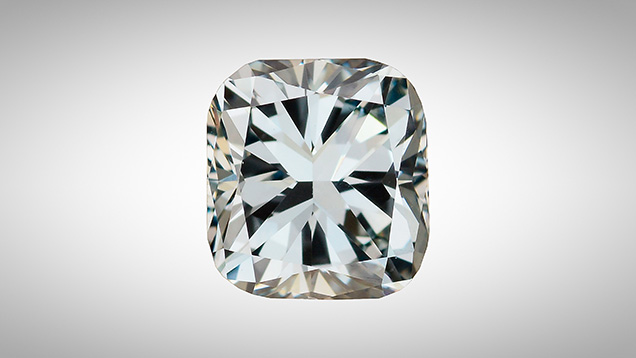
A 0.64 ct Fancy grayish greenish blue cushion modified brilliant (figure 1) was recently found to be a composite of synthetically grown and natural diamond. During testing, the infrared spectrum showed both strong absorption of nitrogen and the absorption of uncompensated boron, features characteristic of type Ia and type IIb diamonds, respectively (figure 2). The UV-Vis-NIR spectrum showed “cape” peaks, which are nitrogen-related defects, but also a sloping absorption into the red portion of the spectrum caused by uncompensated boron. It is very unusual for boron- and nitrogen-related defects to be seen together in natural diamonds, though an example has been seen before (Spring 2009 Lab Notes, pp. 55–57). Mixed-type diamonds always call for additional scrutiny.
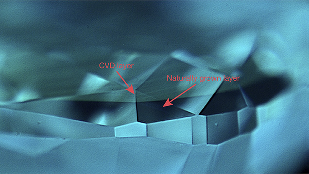
The DiamondView fluorescence image taken on the pavilion showed a blue hue, caused by luminescence from the N3 defect, and natural growth features. The image taken on the crown showed a greenish blue color common to boron-bearing diamonds and the dislocation patterns characteristic of CVD-grown diamonds. In the image taken from the side, a layer can be seen between the natural substrate and the CVD-grown addition (figure 3). These two distinct fluorescence patterns—the greenish blue from the CVD layer and the darker blue from the naturally grown layer—prove that a layer of CVD synthetic diamond was grown on a natural substrate. A wireframe model generated from a non-contact optical measurement device was uploaded to the DiamCalc diamond modeling program. Using the fluorescence images as a guide, we obtained a 3D section that represented only the CVD layer. From this, we calculated an approximate layer weight of 0.10 ct and a thickness of approximately 200 microns. A similar diamond previously reported was also a type IIb CVD layer grown on a natural Ia substrate (Summer 2017 Lab Notes, pp. 237–239). That composite was Fancy blue, weighed 0.33 ct, and had a CVD layer that was 80 microns thick.
When viewed through a microscope, small pinpoint-like polish features were observed from facet to facet along with a faint line resembling surface graining. These polish features were visible along the entire area of this division and correlated with the separation plane seen in the fluorescence images. Examination with an electrical conductivity tester showed that the crown was conductive but not the pavilion. This is consistent with a type IIb crown and type Ia pavilion.
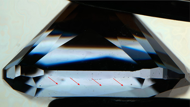
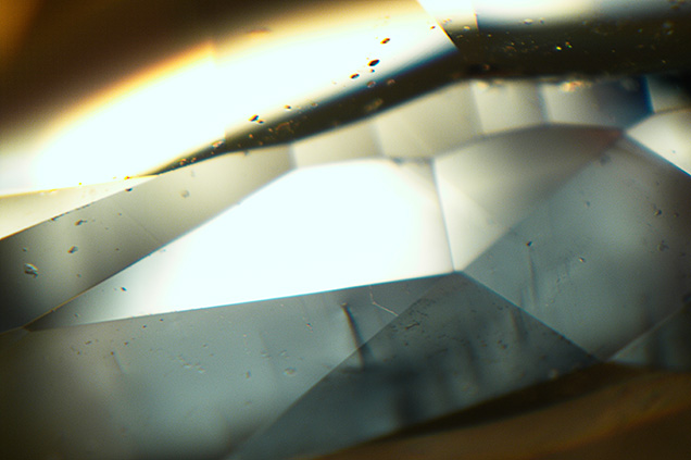
In immersion, the CVD layer was grayish blue whereas the natural substrate had a yellowish bodycolor (figure 4). The blue color in the CVD layer is from the uncompensated boron, and the yellowish color in the substrate is due to the “cape lines” in the visible spectrum. The final color, Fancy grayish greenish blue, is caused by the gray and blue components from the CVD layer and the yellow from the substrate. The resulting color was likely the main motivation for growing the CVD layer on top of the natural diamond, though the extra weight gained could also be a factor. Viewing under crossed polarizers in immersion revealed dislocation bundles that started at or near the interface and grew upward and outward (figure 5). This proves that it was a thick CVD layer and not a coating of CVD overgrowth.
In CVD-grown diamonds, there is some indication in PL spectra that the diamond has been grown in a laboratory—usually the presence of the silicon doublet peak at 736.5 and 736.9 nm or the 596/597 nm defect. Numerous PL spectra were collected in standard and confocal mode on both the crown and pavilion of the diamond in search of any indication of this synthetic overgrowth. In this case, neither of these CVD features were evident, likely due to the thinness of the layer.
With the second of these composites seen at GIA, this could be a new type of product entering the market. Earth-grown diamonds with synthetic diamond grown on the surface require extra scrutiny due to the presence of natural-looking features, both spectroscopic and gemological. Careful inspection still reveals the presence of synthetic indicators, which expose the true nature of the diamond.

A 0.64 ct Fancy grayish greenish blue cushion modified brilliant (figure 1) was recently found to be a composite of synthetically grown and natural diamond. During testing, the infrared spectrum showed both strong absorption of nitrogen and the absorption of uncompensated boron, features characteristic of type Ia and type IIb diamonds, respectively (figure 2). The UV-Vis-NIR spectrum showed “cape” peaks, which are nitrogen-related defects, but also a sloping absorption into the red portion of the spectrum caused by uncompensated boron. It is very unusual for boron- and nitrogen-related defects to be seen together in natural diamonds, though an example has been seen before (Spring 2009 Lab Notes, pp. 55–57). Mixed-type diamonds always call for additional scrutiny.
The DiamondView fluorescence image taken on the pavilion showed a blue hue, caused by luminescence from the N3 defect, and natural growth features. The image taken on the crown showed a greenish blue color common to boron-bearing diamonds and the dislocation patterns characteristic of CVD-grown diamonds. In the image taken from the side, a layer can be seen between the natural substrate and the CVD-grown addition (figure 3). These two distinct fluorescence patterns—the greenish blue from the CVD layer and the darker blue from the naturally grown layer—prove that a layer of CVD synthetic diamond was grown on a natural substrate. A wireframe model generated from a non-contact optical measurement device was uploaded to the DiamCalc diamond modeling program. Using the fluorescence images as a guide, we obtained a 3D section that represented only the CVD layer. From this, we calculated an approximate layer weight of 0.10 ct and a thickness of approximately 200 microns. A similar diamond previously reported was also a type IIb CVD layer grown on a natural Ia substrate (Summer 2017 Lab Notes, pp. 237–239). That composite was Fancy blue, weighed 0.33 ct, and had a CVD layer that was 80 microns thick.

When viewed through a microscope, small pinpoint-like polish features were observed from facet to facet along with a faint line resembling surface graining. These polish features were visible along the entire area of this division and correlated with the separation plane seen in the fluorescence images. Examination with an electrical conductivity tester showed that the crown was conductive but not the pavilion. This is consistent with a type IIb crown and type Ia pavilion.

In immersion, the CVD layer was grayish blue whereas the natural substrate had a yellowish bodycolor (figure 4). The blue color in the CVD layer is from the uncompensated boron, and the yellowish color in the substrate is due to the “cape lines” in the visible spectrum. The final color, Fancy grayish greenish blue, is caused by the gray and blue components from the CVD layer and the yellow from the substrate. The resulting color was likely the main motivation for growing the CVD layer on top of the natural diamond, though the extra weight gained could also be a factor. Viewing under crossed polarizers in immersion revealed dislocation bundles that started at or near the interface and grew upward and outward (figure 5). This proves that it was a thick CVD layer and not a coating of CVD overgrowth.

In CVD-grown diamonds, there is some indication in PL spectra that the diamond has been grown in a laboratory—usually the presence of the silicon doublet peak at 736.5 and 736.9 nm or the 596/597 nm defect. Numerous PL spectra were collected in standard and confocal mode on both the crown and pavilion of the diamond in search of any indication of this synthetic overgrowth. In this case, neither of these CVD features were evident, likely due to the thinness of the layer.
With the second of these composites seen at GIA, this could be a new type of product entering the market. Earth-grown diamonds with synthetic diamond grown on the surface require extra scrutiny due to the presence of natural-looking features, both spectroscopic and gemological. Careful inspection still reveals the presence of synthetic indicators, which expose the true nature of the diamond.

